Current situation and future of LED industry chain
Introduction: The recent development of light-emitting diodes (LEDs) has led to the rapid growth of the lighting industry. Solid-state lighting technology is increasingly penetrating different market segments, such as automotive lighting, indoor and outdoor lighting, medical applications, and household products.
First, LED market development track
According to a recent report from the U.S. Department of Energy, the technology is expected to reduce the lighting industry's energy consumption by 15% by 2020 and 30% by 2030 -- 261 TWh (terawatt hour) of energy savings in 2030 alone, worth more than $26 billion at current prices and equivalent to the current energy consumption of 24 million U.S. homes. In addition, these energy savings used in hybrid power plants will reduce greenhouse gas emissions by about 18 million tons of CO2.
Although in many cases the initial cost of these devices is still higher than that of existing light sources, the greater efficiency and longer life of LEDs makes them competitive. Strategies Unlimited estimates that 400m LED lights were sold worldwide in 2013 and McKinsey research suggests that LEDs will account for 45% of the global general lighting market by 2016 and nearly 70% by 2020. The market is expected to reach $72 billion by 2020, up from about $26 billion today.
The LED unit is a complex multi-component system that adjusts performance characteristics to specific requirements. The following sections discuss white leds and other applications.
1. The development road of LED
The phenomenon of electroluminescence in inorganic materials is the basis of LED luminescence. HenryRound and Oleg Vladimirovich Losev reported the phenomenon of LED luminescence in 1907 and 1927, respectively, in which an electric current passes through a silicon carbide (SiC) crystal to glow. These results have led to further theoretical studies of semiconductor and p-n junction photoelectronic processes.
In the 1950s and 1960s, scientists began to study the electroluminescence properties of Ge, Si and a range of III-V semiconductors (such as InGaP and GaAlAs). Richard Haynes and William Shockley demonstrated that recombination of electrons and holes in p-n junctions leads to luminescence. Subsequently, a series of semiconductors were studied, culminating in the development of the first red light LED by Nick Holonyak in 1962. Under its influence, George Craford invented orange LEDs in 1971, followed by yellow and green LEDs (both made up of GaAsP) in 1972.
Intense research quickly led to the commercialisation of LEDs that glow across a wide spectrum, from infrared to yellow, mainly for use in telephone or control panel indicators. In fact, these LEDs are inefficient and have a limited current density, making them too low for ordinary lighting.
2. Blue Light LEDs
Efficient blu-ray LEDs took 30 years to develop because there were no wide-gap semiconductors of sufficient quality available for use. In 1989, the first SIC-based blu-ray LEDs were commercialized, but SiC was an indirect band-gap semiconductor, making its efficiency very low. The use of direct bandgap semiconductor GaN had been considered since the late 1950s, and in 1971 JacquesPankove demonstrated the first Gan-based LED emitting green light. However, techniques for the preparation of high quality GaN single crystals and the introduction of N-type and P-type doping into these materials remain to be developed.
The development of metal-organic gas phase epitaxy (MOVPE) in the 1970s was a milestone in the development of efficient blue LEDs. In 1974, Japanese scientist Isamu Akasaki began to grow GaN crystals using this method, and in collaboration with Hiroshi Aman, high quality device grade GaN was first synthesized by MOVPE method in 1986.
Another major challenge is the controlled synthesis of P-doped GaN. In fact, during MOVPE, Mg and Zn atoms can enter the crystal structure of the material, but often combine with hydrogen to form an ineffective P-type doping. Amano, Akasaki and their collaborators observed that Zn-doped GaN emit more light after scanning electron microscopy.
In the same way, they demonstrated that electron beam radiation has a beneficial effect on the doping properties of Mg atoms. Subsequently, Shuji Nakamura proposed that a simple post-deposition step was added after thermal annealing to decompose the Mg and Zn complex bodies, which could easily achieve P-type doping of GaN and its ternary alloys (InGaN, AlGaN).
It should be pointed out that the energy band of these terpolymer systems can be adjusted by the composition of Al and In, which adds a degree of freedom to the design of the Blu-ray LEDs, which is of great significance for improving their efficiency. In fact, the active layer of these devices currently usually consists of a series of alternating narrow-gap InGaN and GaN layers and wide-band P-doped AlGaN films (which act as the P-terminal constraint of the carrier).
In 1994 Nakamura and collaborators demonstrated for the first time InGaN Blue LEDs with 2.7% external quantum efficiency (EQE) based on a symmetrical double hetero structure of Zn-doped InGaN active layer between N-type and P-type doped AlGaN (Box 1 lists the main performance index definitions of leds).
The LED structure is illustrated in Figure 1a. These results were critical to the LED-based lighting technology used today and thus revolutionized the lighting industry. In late 2014, the Nobel Prize in Physics was awarded to Akasaki, Amano and Nakamura for "the invention of highly efficient blue leds for lighting and energy saving of white light sources."
3. LED performance index
The Quantum efficiency (IQE) in the material is the ratio of the number of electron-hole recombination (i.e. photon production) radiated to the total recombination (radiation and non-radiation).
This index determines the luminescence efficiency of semiconductor materials. Semiconductor LED performance is usually expressed using external quantum efficiency (EQE), which is the product of IQE and extraction efficiency. Extraction efficiency refers specifically to the fraction of photons produced that escape the LED. EQE depends on semiconductor layer defects that directly affect IQE and device construction that affects extraction efficiency.
Luminous efficacy: Luminous efficacy indicates the efficiency with which a light source emits visible light radiation, and is generally measured in lm W? 1. The light source converts 100% electric energy with monochromatic green light (frequency 4501012 Hz, corresponding wavelength about 555nm, the most sensitive light of human eyes, FIG. 2b shows the corresponding eye sensitivity curve), and its maximum luminous efficiency reaches 683 lm W? 1.
White light sources for illumination usually require a wider emission spectrum than the full range of visible light bands, so their luminous efficiency is significantly lower than its maximum. Electrical energy is converted into radiation outside the eye's sensitivity curve, which cannot be used for lighting and should be minimized.
Correlated colour temperature: Reference sources used to compare different lighting technologies would be black-body radiation, at thermal balance. According to Plancks law of radiation, the emission spectrum of a black-body incandescent lamp depends on its temperature, and the corresponding color points of radiation at different temperatures are represented by CIE diagram, which is called the black dot curve of Planckian locus (FIG. 2f and h).
The relative color temperature (CCT) of white light can be roughly divided into "warm white" (2,500-3,500 K), "natural white" (3,500 -- 4,500 K), "cold white" (4,500 -- 5,500 K), and daylight (5,500 -- 7,500 K) at different locations along the Planck locus.
Colour rendering index (SI) : The color rendering index (CRI) is a dimensionless measure that describes the ability of a white light source to produce color in a manner that is accurate and comfortable relative to human visual perception, taking into account reference light sources (blackbody radiation was tested under CCT<6,000 K or natural light CCT>6,000 K for the same CCT).
Cris are usually defined as the average color rendering of eight test color samples (R1-R8), rated between 0 and 100. For high CRIs an additional R9 value is used, indicating a deep red color. CRI=100 means that all color samples illuminated by the test light source have the same color as the same sample illuminated by the reference light source.

-
Figure 1. Design of Blu-ray InGaN LED chip
a. Schematic of the first blue Light InGaN/AlGaN LED.
b. Schematic diagram of inverted LED chip with inverted structure and non-contact front surface. The two contact points are welded to the substrate near the LED.
c. Schematic diagram of the highest level of thin-film flip LED and top view of LED devices. The effective layers of these three schemata simplify the representation of the double heterostructure, single or multiple quantum well structure InGaN/AlGaN.
Over the past 20 years, the EQE of blue leds has gradually increased, which is also the result of the continuous reduction of GaN crystal structure defect density. The material is usually grown on sapphire substrates for cost effective reasons, however there is a 16% lattice mismatch and different coefficient of thermal expansion. These two factors lead to the generation of dislocation defects during GaN growth of MOVPE near 1,000ˇć.
Careful optimization of the growth process can keep defects in the range of 107 to 108 cm-2, but further improve the quality of semiconductors of the same structure for other LED applications. Although InGaN LEDs have high defect density, they have higher efficiency than other wide-band gap semiconductor diodes (such as ZnSe) with low defect density. The specific reason is still unknown.
Another factor that strongly influences the extraction efficiency and IQE of LEDs is the structure of the devices. Figure 1a shows the outer P-type GaN layer, which has a relatively low conductivity that limits hole injection in the device, but this bottleneck can be overcome by larger P-type contacts covering the entire p-GaN surface. However, electrical contact prevents the output of photons.
Several design options can solve this problem, as shown in Figures 1b and c. Flip chip (FIG. 1b) is when the chip is installed upside down with p- and n- contacts at the back. This configuration provides better heat dissipation and a higher current density, resulting in higher light output per chip surface. Sapphires are transparent in areas of blue and green light and do not prevent luminescence.
In addition, a coating (such as Ag) may be applied to the contact site to reflect those photons emitted towards the base. The thin-film chip flip method (FIG. 1c) can be used to further improve the performance. The substrate is removed from the n-GaN layer and the surface is roughened to improve the efficiency of light extraction. It has been reported that the InGaN LEDs emitting at ~ 44nm have an EQE of 84.3% at 20mA based on the development of materials and structures.
4. From blue to white
The invention of the high-efficiency blue light-emitting diode was a milestone for today's ubiquitous white LEDs. LEDs have higher energy efficiency than traditional light sources and more importantly can be adjusted to suit different applications, such as stage lighting, building lighting and so on.
In general, white LEDs can be obtained by several different methods. One is a combination of three different semiconductor LEDs that emit blue, green and red light (Figure 2a, left). The biggest challenge of this approach lies in the relatively low EQE of green-light semiconductors (ˇÖ25%), which limits the luminous efficiency of corresponding white leds (Figure 2c). InGaN's solid solution with a high content of indium is commonly used to emit green light directly. The lattice mismatch between the substrate and InGaN increases with the increase of indium content, resulting in a higher defect density. In addition, the quantum mechanical Stark effect, which describes the change in electron density distribution around the nucleus, is more pronounced with increasing indium content, which reduces EQE in the green band.
To avoid this limitation, green fluorescent conversion LEDs (pc-LEDs), which basically convert luminous materials, directly use blue leds to emit green light, often replacing green semiconductors in commercial products (FIG. 2a right, FIG. 2c). The typical luminescence spectra of these hybrid leds are shown in FIG. 2b.
These hybrids (direct blue and red plus PC-green light) have significantly improved luminous efficiency and can achieve high color rendering index (CRI) values. The color stability of the red, green and blue (RGB) LEDs is poor due to their different spectral drift and different thermal degradation rates over time.
Complex and expensive circuits that can independently control each channel in RGB need to compensate for this unwanted effect, so the use of these constructs in white-light applications is limited. For functional lighting, as well as for object and architectural lighting, additional electronic components that provide color mixing (dynamically changing the tone of the output color) are very promising.
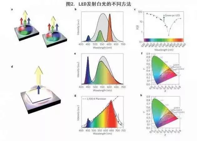
Figure 2. Different ways for leds to emit white light
a. Diagram of white LEDs. Left: Three direct-emitting LEDs (Blu-ray, InGaN; Green light, InGaN; Red Light, AlInGaP). Right: Two direct-emitting LEDs (Blu-ray, InGaN; Red light, AlInGaP) and a green pc-LEDs.
b. Luminescence spectra of white LEDs composed of leds emitting directly blue and red light and a green pc-LED. Gray shadow line: human eye sensitivity curve.
c. External Quantum Efficiency (EQE) of semiconductor LEDs. Blue cube, InGaN base LEDs; Red triangle, Alingap-based LEDs; Green square, green light pc-LED.
d. Schematic diagram of white pc-LED and blue InGaNLED for converting luminescent material on coating.
e. Luminescence spectra of white pc-LED with broadband yellow fluorescence.
f. Blackbody curves (solid black dot lines) and CCT values drawn by the International Commission on Lighting (CIE, 1931). The white squares represent CIE color coordinates for direct blue leds and yellow luminous materials (YAG:Ce). All perceived colors are available along the dot lines of the pc-LED.
g. Luminescence spectra of pc-LEDs with CCT=2,700 K. Black line: narrow band red Sr[LiAl3N4]:Eu2+ LED (CRI=98, R9>90). White dashed line: Sr[LiAl3N4]:Eu2+ luminous summary. Purple curve: Commercial LED (CRI = 96, R9>80). The LEDs showed a good matching relationship with 2,700 K blackbody radiation (black dotted lines). However, PC-leds with narrow red light materials have significantly reduced overflow (black down arrow) in the infrared region.
h. CIE drawing. The white squares represent the CIE color coordinates (Sr[LiAl3N4]:Eu2+) of direct blue leds, yellow luminescent materials (YAG:Ce), and extra red fluorescence. Pc-LED adds blend to get all the colors, represented by triangles. Here, almost all CCT values for the blackbody curve (solid black line) can be obtained.
According to the color mixing principle (FIG. 2d), a simple way to provide white light based on the pc-LED strategy is to combine a single blue-light InGaN chip with one or more light-emitting materials in the visible region. Following this strategy, the first commercial white pc-LEDs developed by Nichia back in 1996 used Ce3+ doped garnet materials (e.g. Y3? xGdxAl5? yGayO12:Ce3+(YAG:Ce)) to emit wide-spectrum yellow light (FIG. 2e, f). Only a single fluorescence is used, limiting the performance of CRI<75 light sources in the cold white and daylight ranges (CCT=4,000-8,000 K). However, high conversion efficiencies close to theoretical limits make these devices an important component of vehicle headlights that require a CCT value comparable to daylight (~6,400 K).
Lighting applications with ideal natural color perception prefer lower CCT values (2,00-4,000 K) and higher CRIs>80. These parameters are easier to achieve using two or more luminous materials (for example, LuAG:Ce or YAG:Ce of green to yellow light combined with red light (Ba,Sr)2Si5N8:Eu2+ or (Sr,Ca)AlSiN3:Eu2+). By adjusting the ratio of these materials, continuous emission spectra covering the entire visible region close to that of blackbody radiation can be obtained (FIG. 2g, h). However, the highlight quality of CRI>90 (commonly used in museums, medical rooms, retail stores, etc., which require the most natural colors) usually comes at the expense of luminous efficiency. Considering the curve of human visual sensitivity (FIG. 2b), photons after 650 nm are very weak, resulting in a great loss of luminous efficiency. Therefore, compared with PC-leds, which focus more on red light components, PC-leds can be better adapted to visual perception (and have higher luminous efficiency) by fine-adjusting the position and width of the emission spectrum of luminous materials.
5, improve the red luminous materials in white light
The U.S. Department of Energy recently set the 2020 market standard for luminescent white LED efficiency 200Im W-1. Such high efficiency usually requires pc-LEDs to perform under harsh conditions, such as chip surface temperatures of up to 200ˇć (generated by high current density) and fast photon pump rates of the main blue LEDs.
Therefore, appropriate fluorescence is required to exhibit high conversion efficiency, rapid decay, and high thermal degradation resistance under these conditions. Eu2+ doped nitrides such as (Ba,Sr)2Si5N8:Eu2+ (usually the peak center is between ¦Ëem~590 -- 625nm, Half-peak width FWHM is 2,050-2,600cm-1) or (Ca,Sr)AlSiN3:Eu2+ (¦Ëem~610 -- 660nm, FWHM~2,100 -- 2,500cm? 1) Red light material has been used as commercial lighting grade white light pc-LEDs.
However, the relevant part of the emission spectrum is outside the sensitivity range of the human eye (infrared spillover, Figure 2g), limiting the overall luminous efficiency of the device. Sr1? xCaxS:Eu2+ (¦Ëem~615 -- 650nm, FWHM~1,550 -- 1,840cm? 1) and other narrower emission materials have also been tested, but their industrial applications are limited due to their chemical reactions with packaging materials and their limited conversion efficiency as the temperature increases.
Recently, a new class of nitride materials with very narrow red emission has been obtained. In the present study, Sr[LiAl3N4]:Eu2+(¦Ëem =650nm, FWHM~1,180cm? 1) and Sr[Mg3SiN4]:Eu2+(¦Ëem=615nm, FWHM~1,170cm? 1) leds as the basis for the next generation of lighting pc-LEDs.
Sr[LiAl3N4]:Eu2+ has good thermal performance and can reduce infrared emission for low CCT and high CRI applications (e.g. CCT=2,700K, CRI>90). LEDs with high CRI are expected to increase the luminous efficiency by 4-12% compared with commercial LEDs (FIG. 2g). Further improvements are expected by shifting the red emission spectrum to a shorter wavelength (~ 600-630nm), preferably with a narrower emission band.
GE's recently commercialized Mn4+ doped fluoride is another class of narrow red light emitting materials. Several sharp lines (each less than 5nm) appear near 630 nm in the emission profiles of these materials. When combined with green-yellow luminous garnet material, lamps with high CRI and high luminous efficiency are obtained. However, the long luminescence decay time of Mn4+ and the low thermal stability of ionic fluoride donor materials are likely to limit the practical application of these phosphors to produce relatively low current density and low heat.
Finally, hybrid devices combining direct red emission LEDs and complementary pc-LEDs can also be used as high quality lighting. However, the temperature sensitivity of direct red leds requires more complex structural designs and limits their application to low thermal constraints, such as non-directional lighting over large areas.
6. Improve LCDs green transmitter
LEDs are widely used in modern liquid crystal display (LCD) backlight components. In these devices, leds emit light through a polarization filter, a layer of liquid crystals, a color filter, and a secondary polarization filter (FIG. 3a). The transmittance of polarized light passing through the two-stage polarization filter depends on the orientation of the liquid crystal and can be electrically tuned. Unlike lighting applications, optimal display performance is required.
In particular, the gamut is provided by the LCD display, depending on the CIE (Commission Internationale de l? clairage, usually corrected by a specific Standard (e.g., NationalTelevision Standard Committee (NTSC), CIE 1931). The sensitivity and wavelength-dependent resolution of the human eye are higher in the green light band, so a large number of green tones can be distinguished.
As a result, if the green emitter bandwidth in the backlit LEDs is narrower (FIG. 3b), the colour gamut displayed on the LCD will be significantly increased. The single phosphor pc-LEDs of commonly used garnet materials (such as YAG:Ce with broad band green-yellow composition) cannot meet these requirements, while the red, green and blue LEDs are difficult to apply, especially the EQE of green leds is very low.
The most advanced high-gamut LEDs are a combination of narrow-band green ¦Â-SiAlON:Eu2+(¦Ëem=525nm, FWHM~50nm) and narrow-band red K2SiF6:Mn4+(¦Ëem=613, 631, 636, 648nm, each FWHM<5nm). Especially in smaller displays, such as tablets and some TV models, panels containing narrow green and red emission quantum dots are backlit with a high gamut. The development of solid state materials with narrow emission bandwidths in the green light band will help to improve the maximum displayable color gamut of LCD displays based on energy-saving LED backlights.
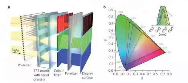
a. LCD display diagram. TFT stands for thin-film transistor.
b. CIE (1931) drawing with different gamut. The black dots represent the NTSC standard chromaticity coordinates. The dashed line represents the NSTC gamut. The white dots represent the chromaticity coordinates of the backlit LED that passes through the corresponding filter (blue, green, red). Depending on the FWHM and spectral peak position of the luminous material, the green value can be assumed to be different positions in the CIE diagram, resulting in different color gamut. The gray triangle represents the color gamut achieved by wide-band green-yellow luminous garnet. The blue and red triangles represent the increased gamut using the narrower green luminous material (see illustration).
Inset: The black curve shows the passband of a typical green filter. The gray, blue and red curves show the emission distribution of the corresponding green luminous element in the CIE diagram.
7. Application prospect
Global sales figures confirm the growing LED lighting market, and expansion in other areas is also anticipated. LEDs have the potential for independent colour adjustment, so their emission performance can be adjusted according to different requirements. Such spectrally controlled lighting can be adapted to physiological responses, such as helping to improve concentration or sleep.
Intensive LED lighting is also having growing medical implications, such as relieving muscle tension or treating skin conditions. In addition, solid-state lighting with specific wavelengths is expected to stimulate photosynthesis and optimize the growth of greenhouse crops. In the field of general lighting, we will continue to benefit from new LED products through the continuous development of cost effectiveness and performance.
Two, LED industry chain
(I) Introduction to LED
1. Basic introduction of LED
LED is the abbreviation for "Light Emitting Diode", translated as "light emitting diode" in Chinese. It is a semiconductor device that converts electrical energy into light energy. The core part of LED is a chip composed of P-type semiconductor and N-type semiconductor. There is a p-n junction between the P-type semiconductor and N-type semiconductor. When the injected few charge carriers are combined with the majority of carriers, the excess energy will be released in the form of light, thus converting electrical energy into light energy. Chips made of different materials can emit red, orange, yellow, green, blue, purple and other colors, hence the name "light-emitting diode".
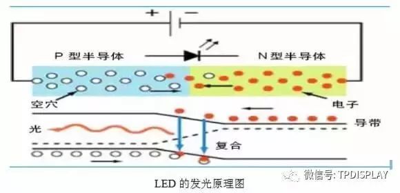
Compared with traditional lighting, LED has obvious advantages in energy saving and is currently the world's advanced lighting technology. It is regarded by the industry as one of the great inventions after Edison invented the incandescent light bulb.
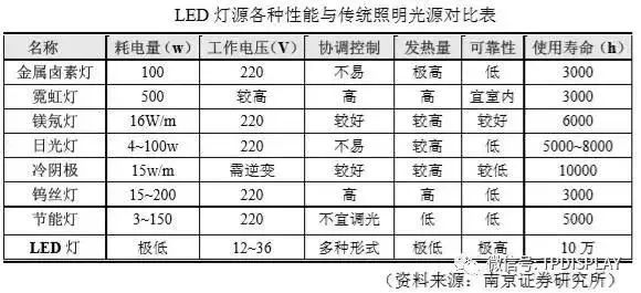
Another feature of leds is that they are environmentally friendly. LED is a solid state light emitting device, which does not contain mercury, and will not cause toxic metal environmental pollution due to rupture during production and use.
2. LED application field and its classification
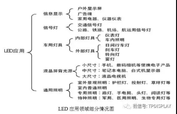
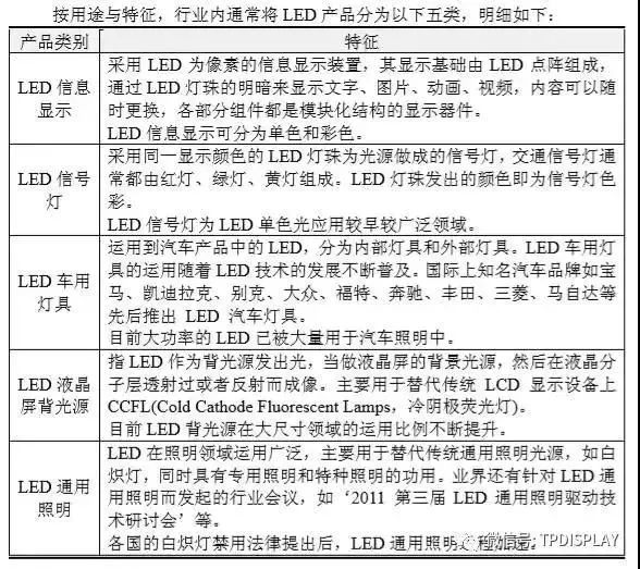
In the context of global energy crisis, energy-saving, environmental protection, colorful, safe, long life, miniaturized semiconductor LED lighting has been recognized as the third lighting revolution in the history of human lighting. With the improvement of LED technology, its application field is constantly expanding and extending, is widely used in LCD screen backlight, general lighting, signal display, traffic lights and car lamps and other fields.
3. LED packaging and product classification

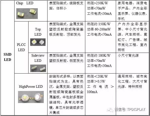
LED packaging refers to the process of wrapping LED chips and scaffolds with materials such as epoxy resin or silicone. Specifically, it is to arrange, fix and connect the LED chip and other components on the bracket or substrate, lead out the terminal, and through the plastic transparent insulator dielectric envelope fixed, constitute the whole three-dimensional structure process, to provide protection and heat dissipation function for the normal work of the chip.
Currently, Lamp and surface mount are the main types of LED devices. Compared with Lamp, SMDS have many unique and excellent characteristics, such as high assembly density, small size of electronic products, light weight, and saving materials, energy, equipment, manpower and time. The concrete embodiment is:
(1) Low defect rate of solder joint, good high-frequency characteristics, reduce electromagnetic and radio frequency interference;
(2) High reliability and strong vibration resistance;
(3) Easy to realize automation, improve production efficiency, reduce the cost up to 30%-50%;
(4) The volume and weight of the patch components are only about 1/10 of the traditional plug-in components. Generally, after SMT is adopted, the volume of electronic products will be reduced by 40%-60% and the weight will be reduced by 60%-80%.
At present, SMD LED is mainly used in backlight, lighting and other fields.
Differentiated from the packaging form, SMD LED products include Chip class, Top class, Sideview class and high-power class products, among which TOP class, Sideview class and high-power class products mainly white light, highlighting, the main application field for backlight (such as: mobile phone, computer and other fields) and lighting (such as: Indoor lighting, outdoor lighting, etc.). Therefore, the specific products packaged in the high-end form of SMD are usually TOP products, Sideview products and high-power products, which are specifically manifested as white light and highlighting products. The domestic in-line device market has been basically saturated, and the profit has been declining year by year. The competition of low-end SMD devices has become increasingly fierce, and the production capacity of middle and high-end SMD devices is in the stage of gradual release. The product price changes greatly.
4, LED according to the luminous color classification and application
LED belongs to the category of semiconductor photoelectric devices, which can be divided into monochromatic LED, full-color LED and white LED according to the luminous color. Among them, white LED is mainly used in the field of backlight and lighting, with a wide range of uses. The classification and application fields of each color LED are as follows:
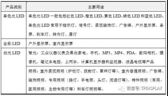
With the improvement of luminous efficiency of white LED, semiconductor lighting has been widely used in mobile phones, backlight, special lighting and other fields, and is advancing to the field of general lighting. Plan according to the U.S. Semiconductor Lighting Development Blueprint (OIDA2002.11) (Source: "China Semiconductor Lighting Industry Development Yearbook" (2008-2009)), by 2012 the luminous efficiency of LED lighting to reach 150lm/w, 2020 luminous efficiency of LED lighting to reach 200lm/w, penetration into all lighting fields. At present, the luminous efficiency of white LED is about 120lm/w. Constantly improving the luminous efficiency of white LED has become one of the important contents to promote the progress of white LED technology. So far, no product has been found that is more suitable for semiconductor lighting than white leds.
5. Overview of LED application development
As early as 1907, human beings discovered the phenomenon of electrified luminescence of semiconductor materials. However, it was not until the 1960s that red light LED made of compound semiconductor material GaAsP was really commercialized. However, due to the very low luminous efficiency and very high cost, it was only used for a variety of expensive electronic equipment signal indicator.
Since the 1990s, with the gradual improvement of LED luminous efficiency and intensity, as well as the full coverage of luminous color to the whole visible spectrum, the energy-saving effect and practicability of LED light source have been highlighted, and its application field has been greatly expanded. At present, LED has been widely used in LCD screen backlight, outdoor large screen, optical communication light source, traffic lights, stage lights, landscape lights, automotive taillights, and gradually into the street lamp, indoor lighting, automotive headlights and other traditional lighting applications.
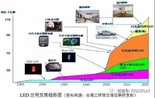
6. Development status of global LED packaging industry
The development of the global LED packaging industry is accompanied by the development of LED industry chain technology, with obvious characteristics of industrial transfer. The world's five leading LED companies, Nichia, ToyodaGosei, CREE, Lumileds and Osram, represent the high technology level of LED and lead the development of LED industry.
In the 1950s, Britain invented the first LED (Light EmittingDiode) with modern significance. In 1962, General Electric Company of the United States was the first to develop the first practical application of visible light emitting diode. By the 1970s, yellow and green LED luminaires were born, and with the invention of new materials and improved light efficiency, the power and luminous flux of individual LED light sources increased rapidly. In the decades that followed, leds developed rapidly, doubling in brightness every 18 months in line with Moore's Law. In the 1990s, the blue LED developed by Japan's Nichiya company drove the successful development of white LED, which made the application of LED take a substantial step from simple sign display function to lighting function.
With the continuous development of technology, LED is breaking through the problems of light decay, heat dissipation, light efficiency, and gradually become recognized as a new type of energy saving and environmental protection light source, with superior economic and social benefits, application prospects are extremely broad. In order to save energy and promote environmental protection, many countries are now stepping up legislation or launching corresponding scientific research and application plans, or making a clear timetable to encourage the use of energy-saving light sources. In July 2001, the U.S. department of energy (doe) start a program called "Next - GenerationLightingInitiative (NGLI)" program, namely "Next generation lighting plan". The Japan 21st Century Lighting Program is a national program initiated and organized by the Metal Research and Development Center of Japan and the New Energy Industry Technology Development Agency (NEDO). In July 2000, EU implemented Rainbow project bringscolorto LEDs and set up Executive Research Agency (ECCR) to support and promote the application of white leds through EU's BRITE/EURAM-3program. In response to the global trend of energy conservation and environmental protection, the Ministry of Commerce, Industry and Energy of Korea has established the "GaN Optical Semiconductor" development program to develop white LED lighting sources based on GaN materials. Since 2000, China has continuously launched a number of LED support policies, and launched the "Ten Cities Ten Thousand Lights" LED lighting promotion plan in 2009 to vigorously develop the LED industry.
The global LED industry has been widely used in various fields and achieved rapid development under the strong support of government policies of various countries. Currently, the global LED packaging industry is mainly concentrated in Japan, Taiwan, the United States, Europe, South Korea and mainland China and other regions. Among them, Japan, the United States, Europe, because of the advantages of the first industrial technology and manufacturing equipment, as the world's early LED packaging industry development regions; Taiwan and South Korea have a complete industrial chain of consumer electronics, clear division of labor in the upper, middle and lower industries, and stable supply and marketing of the industrial chain, so the rapid rise in recent years. Mainland China has cost advantages and rapidly expanding LED application market. In the past 10 years, LED packaging capital from countries around the world, including Taiwan, has been continuously transferred to mainland China, and they have set up packaging factories in mainland China. Domestically-funded packaging enterprises continue to grow and develop, and their technologies continue to mature and innovate. Mainland China has also become one of the regions where LED packaging is rising rapidly.
LED packaging is both technology-intensive and capital-intensive. Due to the cost advantage and the rapidly expanding LED application market in mainland China, international and Taiwan packaging manufacturers have invested and set up factories in mainland China in order to obtain the advantages of nearby supporting and terminal market, which enables the sustained and rapid growth of LED packaging industry in mainland China. It also makes mainland China become an important LED packaging base in the world, which not only expands the market share of Chinese mainland LED packaging in the world LED packaging field, but also improves the LED packaging technology of Chinese mainland manufacturers, and accelerates the rapid development of the entire industry. China's packaging industry has initially formed four LED intensive regions, namely Pearl River Delta, Yangtze River Delta, Fujian-Jiangxi region and Bohai Rim region. China has become an important LED packaging base in the world.
7. Development trend of LED packaging industry
(1) SMD packaging has gradually become the main form of LED packaging
Surface mount packaging SMD LED has become a development hotspot, well solve the problems of brightness, perspective, smoothness, reliability, consistency and so on, the use of lighter PCB board and reflective layer material, in the display reflective layer need to fill less epoxy resin, and remove the heavier carbon steel material pin, by reducing size, reduce weight, It can easily reduce the weight of the product by half, and finally make the application more perfect. It is especially suitable for all kinds of backlight products and indoor and semi-outdoor full-color display applications with decreasing product thickness.
SMD LED packaging has certain technical difficulties, which are reflected in:
One is how to design the structure of the device, optimize the packaging material combination, in order to improve the luminous efficiency of the device, and make the light distribution curve meet the requirements. Good packaging form can not only improve the use of LED chips, but also help enterprises to achieve product differentiation. The continuous research of SMD device structure has brought the continuous development of device structure, and special devices for market segments have been emerging, such as oval LED to meet the requirements of outdoor display applications, and side light LED to meet the requirements of small size LCD backlight.
The second is to effectively solve the problem of heat dissipation, in order to improve the reliability of devices. The high thermal resistance of LED devices will lead to high PN junction temperature of chip, resulting in LED light decay, heat dissipation is the primary technical difficulty of LED packaging. The continuous research of this key technology has enriched and developed the packaging materials, so that the thermal resistance of the device is greatly reduced and the service life of the device is fundamentally guaranteed.
The packaging technology of white LED has become a key technology that the industry pays attention to and puts more research forces into. Advanced packaging technology is used to improve the control of parameters such as color temperature, chrominance coordinate and color development index of white LED, so as to obtain high-quality white LED to meet the requirements of different markets for different white LED. To achieve mass production of white LED color temperature, chromaticity coordinates, color rendering index is highly concentrated, for any manufacturer, is a very challenging technical problem.
(2) Backlight and lighting products will become the driving force for the subsequent rapid growth of the LED market
With the rapid increase in LED backlight penetration in large-size LCD panels and the development of the LED lighting market beyond expectations, the entire LED industry will see accelerated growth momentum. LED backlight and LED universal lighting are two fast-growing areas, and backlight and lighting will be the driving force for the rapid growth of the LED market.
8, backlight LED market demand
LED backlight includes small size backlight, medium size backlight and large size backlight, among which small size backlight is mainly used in mobile phones, MP3, MP4, PDA, digital camera, camcorder and fitness equipment; Medium size backlight, mainly used in laptops, netbooks, computer monitors and monitors; Large size is mainly used in LCD TV and so on.
The number and performance requirements of LED backlight for LCD screens of different sizes are as follows:

9. Lighting LED market demand
Compared with ordinary lighting, LED lighting has the advantages of energy saving, environmental protection, short response time and long service time, so it is an ideal alternative light source. At present, its use cost is high, and its promotion is restricted. However, with the gradual reduction of LED cost, and the promotion of energy-saving policies by governments around the world and the phase-out of incandescent lamps worldwide, LED lighting will bring huge development opportunities. LED lighting application market can be divided into outdoor landscape lighting (guardrail lights, projection lights, lawn lights, etc.), indoor general lighting, decorative lighting, special lighting (street lights, flashlights, headlights, reading lights, etc.), special lighting (military, medical lighting, biological lights, etc.) and car lights.
With the prohibition of incandescent bulbs, business opportunities for LED bulbs below 10W have emerged. According to the current lighting accounts for 19% of global electricity consumption, the total energy consumption reached 2,651 TWH. It is estimated that 30 percent of energy consumption could be saved by replacing existing light sources with energy-efficient ones. An additional 30 percent of energy consumption could be saved by further combining energy-saving light sources with sensors, smart grids and other related applications. A 50 percent reduction in energy consumption by 2030 would be equivalent to saving 2 billion barrels of oil from CO2 emissions.
The global average consumption of incandescent bulbs is 20 billion per year, and each percentage point increase in LED penetration in the incandescent lighting sector will lead to an additional demand of 3.2 billion LED packaging devices.
10. Competition pattern of LED packaging industry in Mainland China
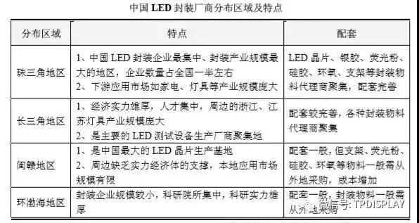
These four regions have been the foundation of the development of China's LED industry and the main areas for the application and promotion of LED products. Among them, the Pearl River Delta region is a region where LED packaging enterprises are concentrated and the packaging industry is large-scale. The number of enterprises accounts for about half of the whole China. This region gathers many manufacturers and agents of packaging materials and equipment, and the supporting system is perfect. Yangtze River Delta, with Shanghai, Hangzhou, Yangzhou and Ningbo as industrial agglomeration centers, has a good investment environment and is the second largest packaging base in China's LED industry, with a balanced upstream and downstream industrial chain. Fujian and Jiangxi areas mainly take Xiamen, Quanzhou, Nanchang and Jingdezhen as the industrial gathering centers, which are the largest epitaxy and chip manufacturing bases in China. Due to its proximity to Taiwan, Fujian and Jiangxi have superior advantages in the connection of LED industry. With Beijing, Shijiazhuang, Shenyang, Dalian and Weifang of Shandong as the industrial agglomeration centers, the Bohai Rim region is characterized by numerous scientific research units, institutes and universities. Therefore, it has always been at the forefront of China in the research of LED process technology and LED equipment.
11. Overview of industrial chain
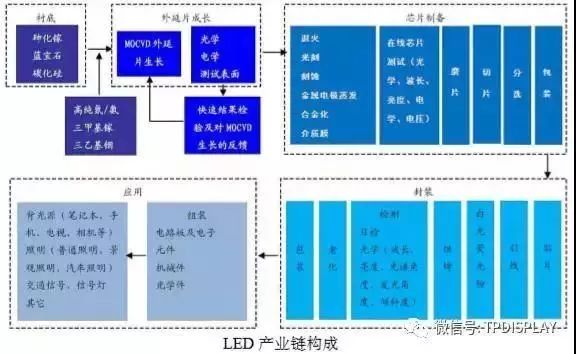
LED industry has a typical unbalanced industrial chain structure, which is generally divided into upper, middle and downstream according to material preparation, chip preparation and device packaging and application. Although there are few industrial links, it involves a wide range of technical fields and diversified technological processes, and the technical characteristics and capital characteristics of each field are very different.
The industrial chain of LED industry can be mainly divided into four parts: LED epitaxial wafer growth, chip manufacturing, device packaging and application products and related supporting industries, which are divided into upstream, midstream and downstream. Semiconductor substrate materials, epitaxial wafer manufacturing is the upstream industry, chip manufacturing is the midstream industry, device packaging and LED device based application product manufacturing is the downstream industry.
12. Production process flow
The packaging process of white LED is realized by adopting high-precision fully automated production equipment, and the packaging environment is 10,000 level dust-free workshop.
A. Production process flow chart of backlight LED devices

B. Production process flow chart of lighting LED devices
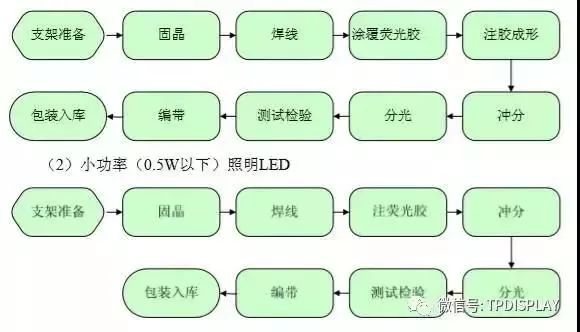
(1) High power (including 0.5W and above) lighting LED
13. Environmental protection
There is no high danger or heavy pollution in the production process, and the products are energy saving and environmental protection products. The main pollution sources and pollutants are: domestic wastewater, general waste gas, organic waste gas, noise sources and solid waste, among which, noise sources come from cutting machines, welding machines and other process equipment, refrigerators, various pumps, cooling towers and air conditioning units, and solid waste is the waste generated in the production process.
14, safe production and health
(1) Reasonable production organization, advanced production process and production technology should be adopted in process design to reduce dangerous and harmful factors to a low degree.
(2) Local exhaust devices shall be set for the process equipment of harmful gases produced in production, and discharge them after meeting the standards to ensure the health of production personnel.
(3) All electrical equipment and distribution equipment shall be safely grounded, and the distribution system shall be equipped with short-circuit protection and over-current protection measures to ensure the safety of electricity use. Use lightning rod for tall buildings. The 380/220V power supply system adopts zero protection to prevent electric shock accidents.
(4) Lightning protection nets shall be set up in major buildings.
(5) There are emergency lighting and safety exits at the entrances and exits of the workshop and in the clean area for evacuation. In case of an accident, personnel can be evacuated quickly.
(6) A series of noise reduction measures should be taken to reduce the noise generated by fans, pumps and other equipment, such as the selection of low noise equipment, vibration reduction foundation, muffler, etc., to ensure that indoor noise meets the requirements of national norms.
Source: Photoelectric and display
